Long-range goal
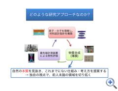
Our principal objective is to develop new functional materials and interfaces that will outperform existing materials, including superconductors, magnetic materials, photo functional materials, ion conductors, and dielectric materials. Our group’s approach combines atom-by-atom engineering with ensemble-measurement techniques. To explore new functional materials, we exquisitely tailor material structures with atomic precision by evaluating both their atomic-scale electronic structures and their macroscopic physical properties. Based on these microscopic and macroscopic properties, we aim to establish future guiding principles for material design and to initiate new fields of research in materials science.
Strategies
 Our strategies to achieve those goals consist of:
- Novel-material synthesis with atomic precision. We focus on designing novel material systems in thin films, heterostructures, low-dimensional structures, surfaces, and interfaces.
- Characterization of the synthesized materials. We use our custom-built analytical instruments to both probe the designed materials’ properties and to elucidate the effects of atomic-scale structure and chemistry on these properties.
- Synergy between analytical results and materials design. We use our experimental results to improve and to design subsequent material systems, until the desired properties are obtained.
Research fields
While applications of designed materials in electronic devices, spintronics, and energy fields have been a major goal in condensed-matter physics, researchers have only begun to utilize oxide nanostructures to design novel functionalities beyond those in surfaces and interfaces. We introduce the concept of “atom-by-atom engineering” of oxide heterostructures, thin films, surfaces, and interfaces to this emerging field. We also extend this approach to other materials including nitrides, hydrides and carbon materials such as graphene. With this approach, we intend to develop future “green materials”.
A. Characterization of electronic states of functional thin films, interfaces, surfaces & exploration of new functional materials
- We have designed and built a low-temperature scanning tunneling microscope with pulsed laser deposition capabilities in ultrahigh vacuum. This unique system enables us to study the local electronic structures of pristine oxide thin films. Using this system, we aim to elucidate the role of the atomic-scale electronic structures of oxide thin films and heterostructures on their macroscopic physical properties. Our current interests also include graphenes, magnetic molecules, and amorphous clusters. Furthermore, we use angle resolved photoemission and transport-measurement techniques as complementary approaches to understanding electronic and magnetic properties of these materials.
![A. 機能性薄膜/界面/表面の電子状態評価と新物質開拓 [新規デバイス開発]](img/research/img_research_02.png)
B. Ion-conducting materials
- Lithium ion batteries are important materials for electric cars and for realizing solar energy society. To this end, high, fast-charging battery capacity remains an essential feature that must be greatly improved. We aim to improve the capacity of Li ion batteries up to ten times that of current Li ion batteries. Since the role of most battery-material physical properties on battery performance are unknown, we synthesize ion-conducting materials by controlling atomic-scale structures (e.g., by controlling the anisotropy of crystals or grain boundaries in heterostructures) to reveal properties relevant to ion conductivity. Our ultimate goal is to elucidate the mechanism of battery operation in the atomic-scale perspective and to open a new frontier for studying electrochemical atom engineering.
Research highlights
Digital Discovery, 4, 1734-1742 (2025).
ACS Appl. Mater. Interfaces, 15, 48 (2023).
APL Mater., 8, 111110 (2020).
Nano Lett., 20, 8200 (2020).
Nano Lett., 15, 1498 (2015).
ACS Nano, ACS Nano 5, 7967 (2011).
Appl. Phys. Lett. 90, 212106 (2007).
Appl. Phys. Lett. 86, 252101 (2005).
Phys. Rev. Lett. 83, 4116-4119 (1999).
Atomic-scale surface migration of a Ga atom on a hydrogen-terminated Si(100)-(2×1)-H surface is
studied using low-temperature scanning tunneling microscopy and first-principles calculations. The Ga atom migrates in a linear potential well confined by adjacent dimer rows and local dihydride defects, and is observed as a continuous linear protrusion (Ga-bar structure) at a narrow range of temperatures near 100 K. The observed height modulation of the Ga-bar structure reflects the local variation in potential energy at individual adsorption sites (adsorption energy variation), which may be caused by the local stress made by surface defects or subsurface impurities.Phys. Rev. Lett. 82, 4034-4037 (1999).


